Trends in Machine Learning Hardware
FLOP/s performance in 47 ML hardware accelerators doubled every 2.3 years. Switching from FP32 to tensor-FP16 led to a further 10x performance increase. Memory capacity and bandwidth doubled every 4 years.
Published
Resources
Executive summary
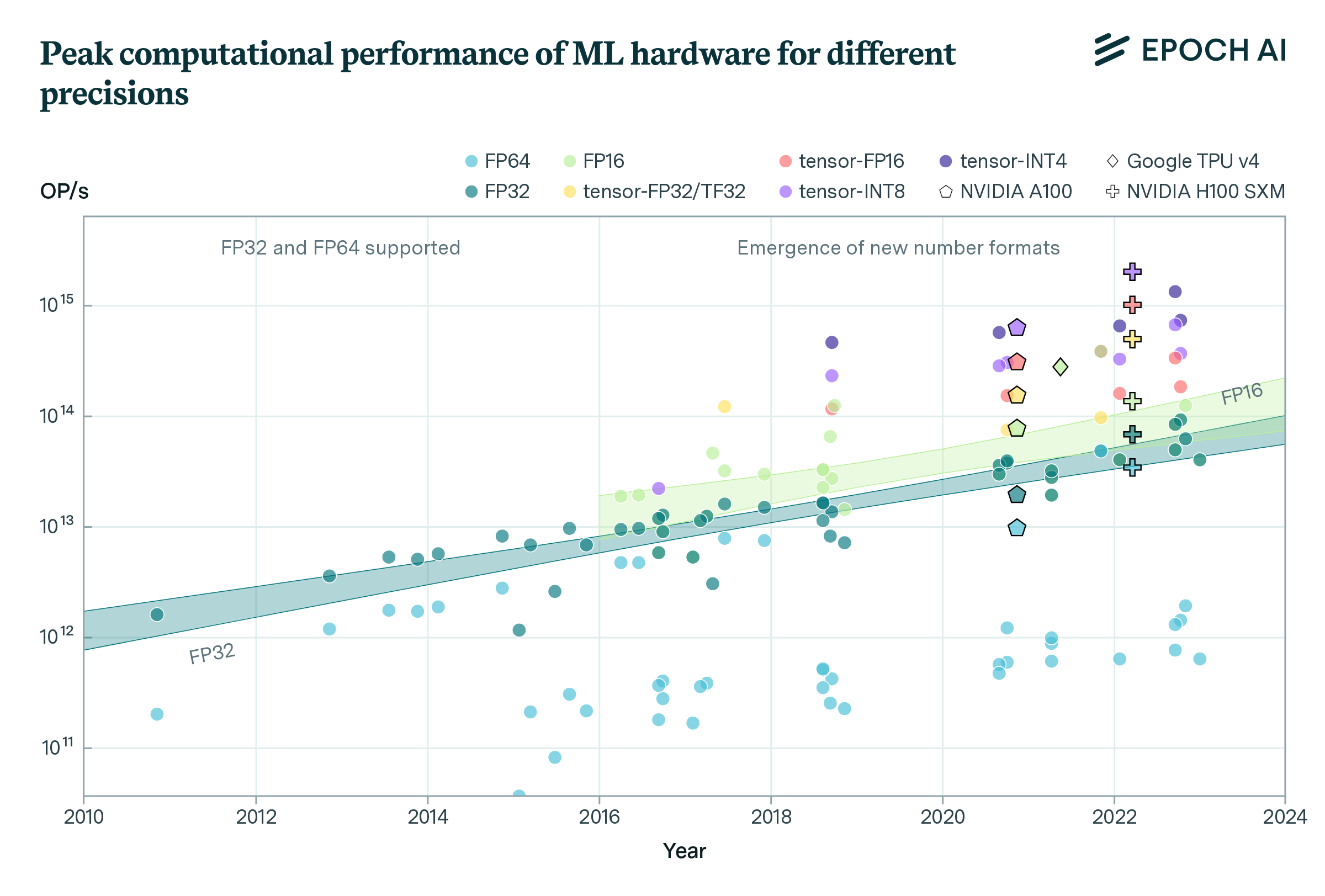
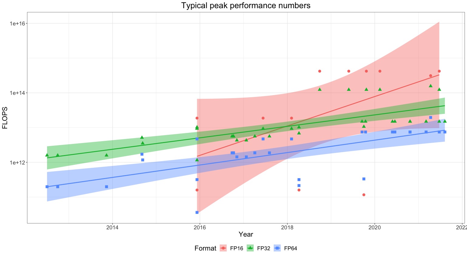
Figure 1: Peak computational performance of common ML accelerators at a given precision. New number formats have emerged since 2016. Trendlines are shown for number formats with eight or more accelerators: FP32, FP16 (FP = floating-point, tensor-* = processed by a tensor core, TF = Nvidia tensor floating-point, INT = integer)
We study the performance of GPU for computational performance across different number representations, memory capacities and bandwidth, and interconnect bandwidth using a dataset of 47 ML accelerators (GPUs and other AI chips) commonly used in ML experiments from 2010-2023, plus 1,948 additional GPUs from 2006-2021. Our main findings are:
- Lower-precision number formats like 16-bit floating point (FP16) and 8-bit integers (INT8), combined with specialized tensor core units, can provide order-of-magnitude performance improvements for machine learning workloads compared to traditionally used 32-bit floating point (FP32). For example, we estimate, though using limited amounts of data, that using tensor-FP16 can provide roughly 10x speedup compared to FP32.
- Given that the overall performance of large hardware clusters for state-of-the-art ML model training and inference depends on factors beyond just computational performance, we investigate memory capacity, memory bandwidth and interconnects, and find that:
- Memory capacity is doubling every ~4 years and memory bandwidth every ~4.1 years. They have increased at a slower rate than computational performance which doubles every ~2.3 years. This is a common finding and often described as the memory wall.
- The latest ML hardware often comes with proprietary chip-to-chip interconnect protocols (Nvidia’s NVLink or Google’s TPU’s ICI) that offer higher communication bandwidth between chips compared to the PCI Express (PCIe). For example, NVLink in H100 supports 7x the bandwidth of PCIe 5.0.
- Key hardware performance metrics and their improvement rates found in the analysis include: computational performance [FLOP/s] doubling every 2.3 years for both ML and general GPUs; computational price-performance [FLOP per $] doubling every 2.1 years for ML GPUs and 2.5 years for general GPUs; and energy efficiency [FLOP/s per Watt] doubling every 3.0 years for ML GPUs and 2.7 years for general GPUs.
| Specification and unit | Growth rate | Datapoint of highest performance | N | |
|---|---|---|---|---|
| Computational Performance | FLOP/s (FP32) | 2x every 2.3 [2.1; 2.6] years 10x every 7.7 [6.9; 8.6] years 0.13 [0.15; 0.12] OOMs per year | ~90 TFLOP/s ~9e13 FLOP/s (NVIDIA L40) | 45 |
| FLOP/s (tensor-FP32) |
NA1 |
~495 TFLOP/s ~4.95e14 FLOP/s (NVIDIA H100 SXM) | 7 | |
| FLOP/s (tensor-FP16) | NA | ~990 TFLOP/s ~9.9e14 FLOP/s (NVIDIA H100 SXM) | 8 | |
| OP/s (INT8) | NA | ~1980 TOP/s ~1.98e15 OP/s (NVIDIA H100 SXM) | 10 | |
| Computational price-performance | FLOP per $ (FP32) | 2x every 2.1 [1.6; 2.91] years 10x every 7 [5; 9] years 0.14 [0.18; 0.10] OOMs per year | ~4.2 exaFLOP per $ ~4.2e18 FLOP per $ (AMD Radeon RX 7900 XTX) | 33 |
| Computational energy-efficiency | FLOP/s per Watt (FP32) | 2x every 3.0 [2.7; 3.3] years 10x every 10 [9; 11] years 0.10 [0.11; 0.09] OOMs per year | ~302 GFLOP/s per W ~3e11 FLOP/s per W (NVIDIA L40) | 43 |
| Memory capacity | DRAM capacity (Byte) | 2x every 4 [3; 6] years 10x every 13 [10; 19] years 0.08 [0.10; 0.05] OOMs per year | ~128 GB ~1.28e11 B (AMD Radeon Instinct MI250X) | 47 |
| Memory bandwidth | DRAM bandwidth in Byte/s | 2x every 4 [3; 5] years 10x every 14 [11; 17] years 0.07 [0.09; 0.06] OOMs per year | ~3.3 TB/s ~3.3e12 B/s (NVIDIA H100 SXM) | 47 |
| Interconnect bandwidth | Chip-to-chip communication bandwidth (Byte/s) | NA | ~900 GB/s ~9e11 B/s (NVIDIA H100) | 45 |
Table 1: Key performance trends. All estimates are computed only for ML hardware. Numbers in brackets refer to the [5; 95]-th percentile estimate from bootstrapping with 1000 samples. OOM refers to order of magnitude, and N refers to the number of observations in our dataset. Note that performance figures are for dense matrix multiplication performance.
Introduction
Advances in machine learning over the last decade have in large part been the result of scaling up the amount of computational resources (compute) used for training (Sevilla et al., 2022), and advancements in hardware performance have played a modest role in this progress. Increased investments in ML R&D (Cottier, 2023) led to scaled-up hardware infrastructure as we move from a small number of chips to massive supercomputers.
This article provides an overview of trends in computational performance across a variety of number precisions and specialized components, such as tensor cores. Furthermore, we analyze additional performance factors such as memory capacity, memory bandwidth, and interconnect bandwidth. Overall, we want to provide a holistic picture of all ML hardware specifications and components that jointly determine practical hardware performance, especially in the era of large ML models.
We used peak performance of various metrics throughout this work for comparison, which we source from the specification sheets from hardware producers.2 Typically, only a fraction of the specified peak computational performance is utilized. This depends on a variety of factors, such as the workload specifications and the limits of other specifications, such as the memory capacity and bandwidth. For example, according to (Leland et al., 2016), for common supercomputing workloads, this might be between 5% and 20%, while in ML training this might range between 20% and 70%, depending on the size of the model, how it is parallelized, and other factors (Sevilla et al., 2022). Nevertheless, peak performance serves as a useful upper bound and standard basis for comparison across different hardware accelerators and generations.
Terminology
- Number representation: We differentiate number representation along three dimensions:
- Bit-length/precision: describes the number of bits used to store a number. This typically ranges from 4 to 64 bits.
- Number format: refers to a specific layout of bits, e.g., integer or floating-point. The number format typically includes the bit-length like in FP32, however, we separate the bit layout and bit-length in our piece.3
- Computation unit: shows if a dedicated matrix multiplication unit is used or not. In this piece, we only differentiate between tensor and non-tensor.
- Hardware accelerator: refers to a chip that accelerates ML workloads, e.g., GPU or TPU. We use the terms chip and hardware accelerator interchangeably as general terms and GPU and TPU when referring to the specialized accelerator.
Dataset
We compiled hardware specifications from two key datasets. The first includes 1948 GPUs released between 2006 and 2021 based on Sun et al., 2019, which we will refer to as the general GPU dataset (based on primarily general GPUs not commonly used in ML training). The second dataset includes only 47 ML hardware accelerators starting in 2010, such as NVIDIA GPUs and Google TPUs, which were commonly used in notable ML experiments (as defined in Sevilla et al., 2022). We have curated the latter dataset ourselves and it will be referred to as the ML hardware dataset or, in short, ML dataset (based on ML GPUs). This dataset is publicly available in our datasheet.
Trends of primary performance metrics
In this section, we present the trends for different number representations, memory capabilities, computational price-performance, and energy efficiency. We briefly explain each metric’s relevance for ML development and deployment, present our findings, and briefly discuss their implications.
Number representations
The numeric representation used for calculations strongly influences computational performance. More specifically, the number of bits per value determines arithmetic density (operations per chip area per second).4 In recent years, hardware manufacturers have introduced specialized lower-precision number formats for ML applications. While FP64 has been common in high-performance computing,5 FP32 performance has been the focus of most consumer applications for the last 15 or so years.
Number formats with less precision have become more prevalent in recent years since low precision is sufficient for both developing and deploying the ML models (Dettmers et al., 2022; Suyog Gupta et al., 2015; Courbariaux et al., 2014). According to Rodriguez, 2020, FP32 remains a most widely adopted number format for both ML training and inference today, with industry increasingly transitioning to lower precision number formats like FP16 and Google’s bfloat16 (BF16) for certain training and inference tasks, as well as integer formats INT8 for select inference workloads.6 Other well-known emerging number formats are the 16-bit standard floating-point format FP16, integer format INT4, and the NVIDIA-developed 19-bit floating-point format TF32.7
Computational performance for FP32 and FP16
Historically, the computational performance trend for FP32 precision has been regular over nearly two decades with a doubling time of 2.3 years, closely in line with the rate associated with Moore’s Law. Over the last few years, especially since 2016, we have seen an emergence of hardware with dedicated support of FP16 precision—increasing the absolute computational performance given the reduced bit length.
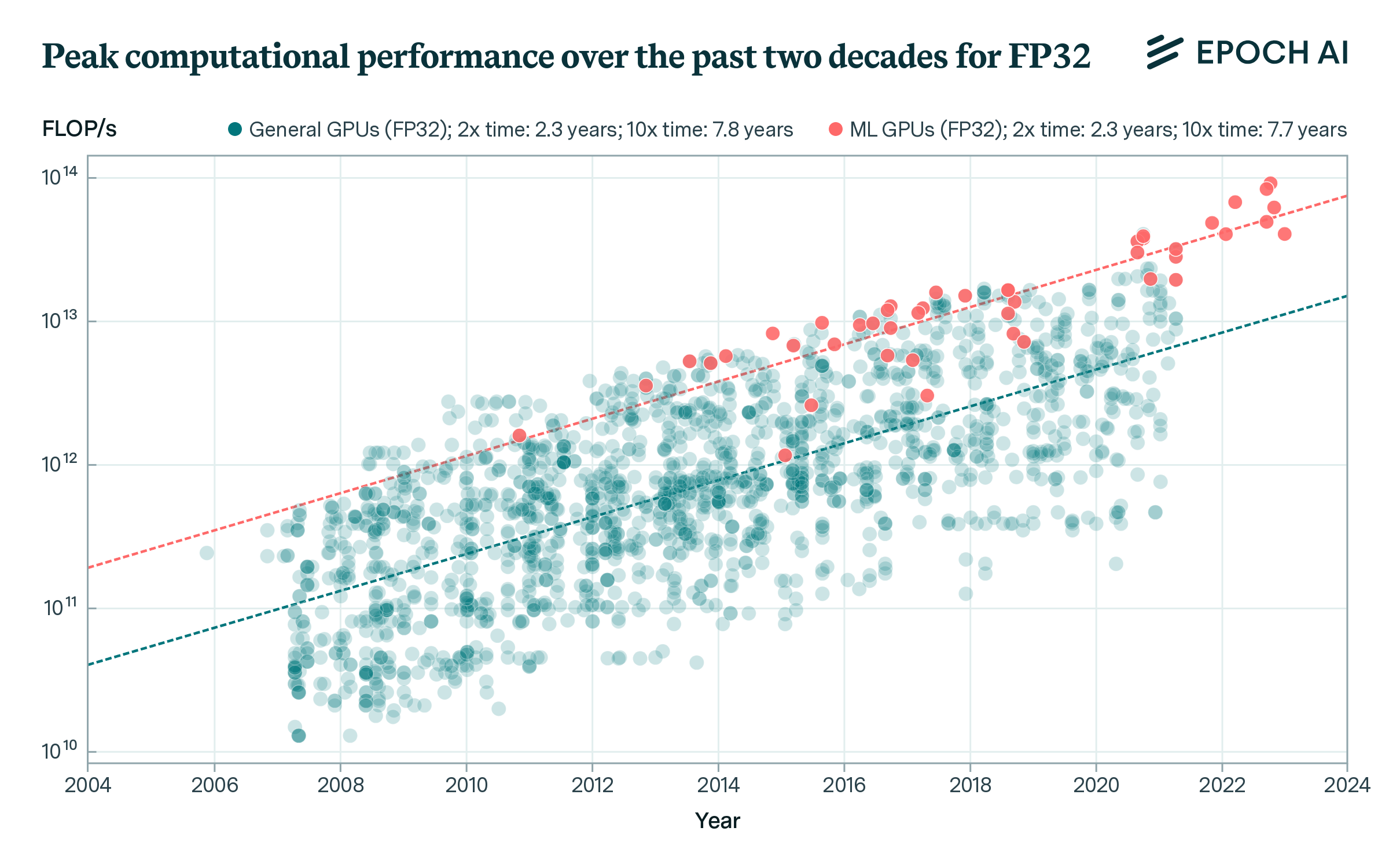
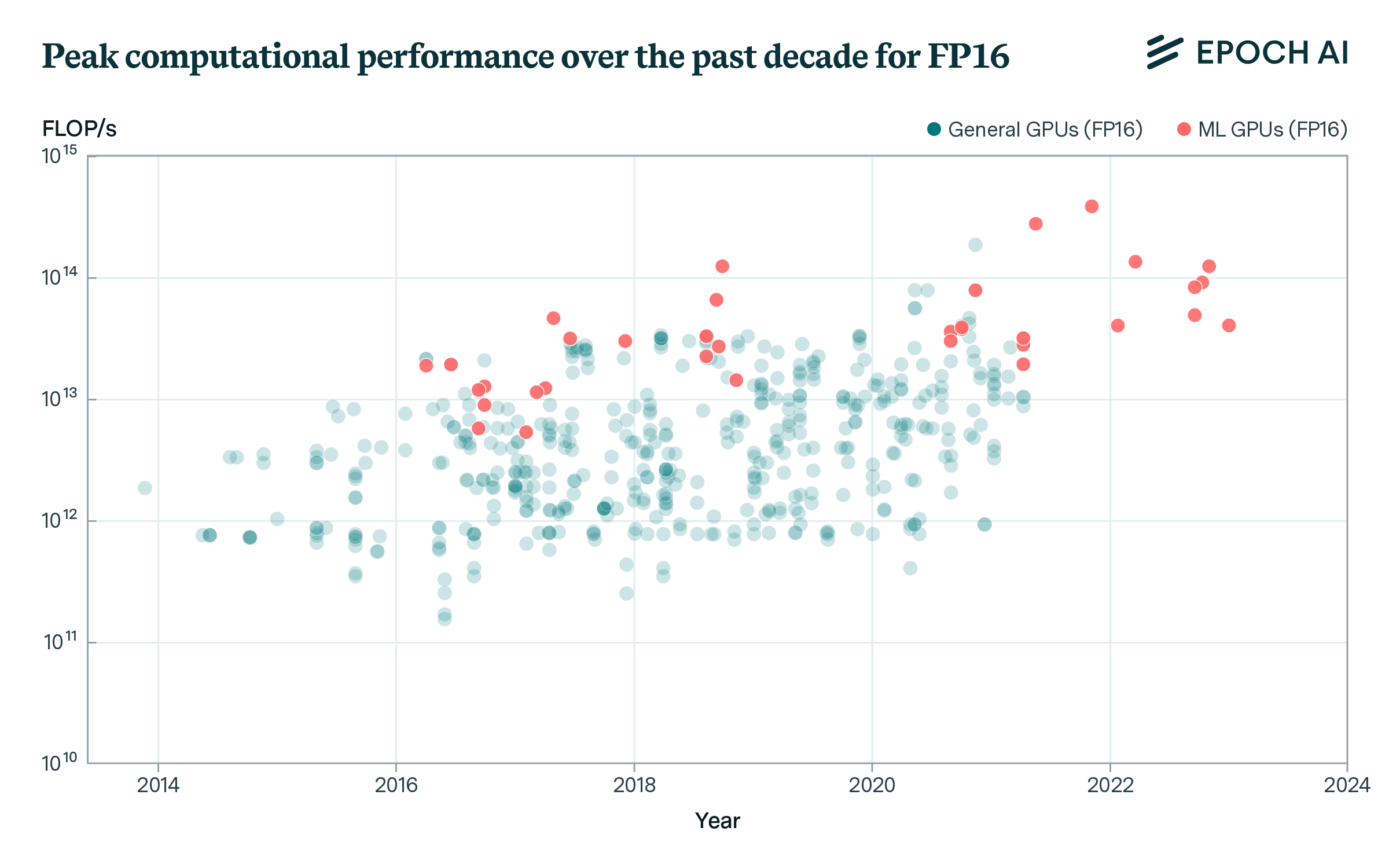
Figure 2: Peak performance of general and ML GPUs for FP32 and FP16 precision over the last two decades. The top figure shows that ML GPUs have a higher median performance than all general GPUs, but the rate of growth is similar. The bottom figure shows that in 2014 some hardware accelerators started to provide FP16 performance details.
The computational performance of general and ML hardware over the last decade for FP32 show nearly identical growth rates but differ in their levels. The accelerators from our ML hardware dataset are consistently among the best available hardware. We think this is in part because ML practitioners selecting the most powerful hardware available and, secondly, the result of the introduction of recent hardware high-end data center GPUs specifically targeting the ML market, e.g., NVIDIA’s V/A/H100 or Google’s TPUs.
Computational performance gains through hardware support for less precise number formats
The performance gains from reduced numeric precision are enabled by multiple architectural improvements in modern ML chips, not just the reduced bit-width alone. The smaller data types allow more FLOPs per chip area and reduce memory footprint. But other advancements also contribute significantly: a) the introduction of new instructions specialized for matrix multiplication,8 b) hardware data compression, and c) the elimination of excess data buffers for matrix multiplication hardware like in NVIDIA A100 (Choquette et al., 20219) which contribute to lower data and instruction memory requirements, leading to more operations per chip area. These advancements are further complemented by faster memory access features in the H100 (Choquette, 2023).
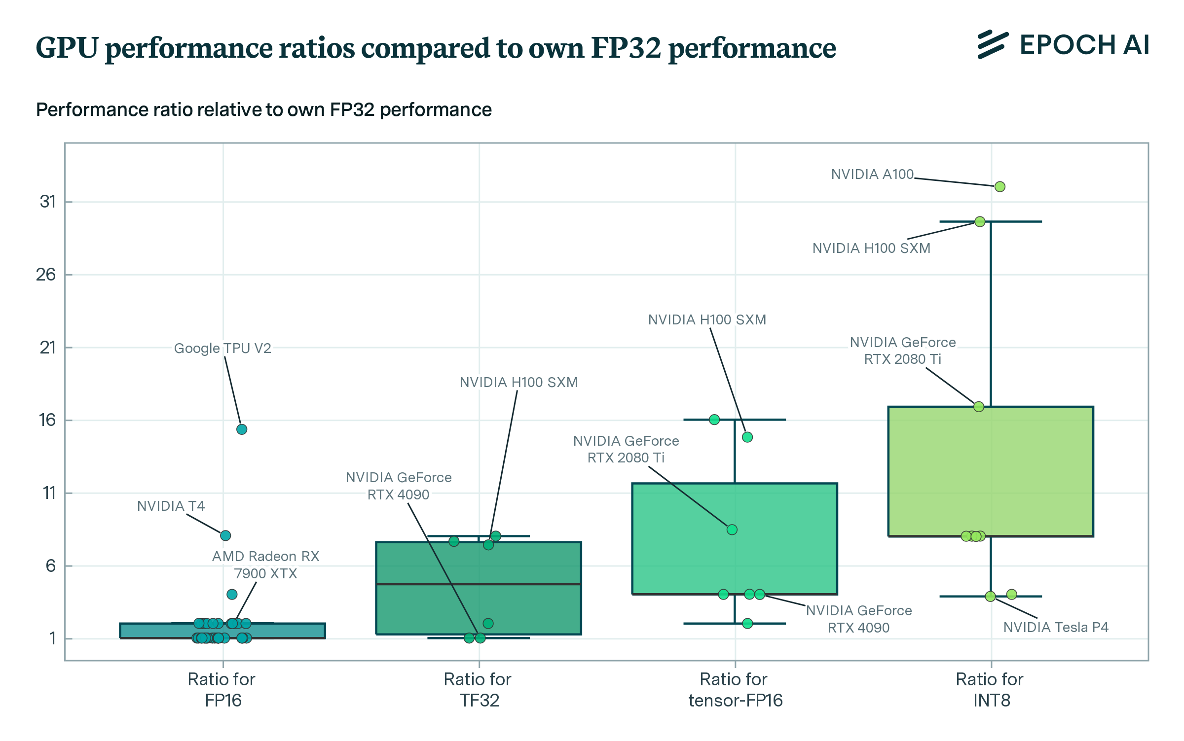
Figure 3: Box plot showing performance of ML accelerators across different precision number formats as a ratio of their own FP32 performance. This illustrates the improvement in performance compared to FP32. We find that new number representations tensor-FP32/TF32, tensor-FP16, tensor-INT8, can increase average computational performance by ~5x, ~8x, ~13x relative to their own FP32 performance respectively. Not all GPUs have dedicated support for lower-precision formats. We removed from this figure all models of GPUs for which computational performance on lower-precision formats was not higher than on higher-precision formats to screen off GPUs without dedicated support.
GPU performance for ML workloads has substantially improved in recent years thanks to lower numeric precision. On average, using lower precision number formats like tensor-FP32 (TF32), tensor-FP16, tensor-INT8 and tensor-INT4 provides around ~5x, ~8x, ~13x and ~18x higher computational performance respectively compared to using FP32 on the same GPU. To put this in context, given that peak FP32 performance has historically doubled every ~2.3 years, these lower precision speedups are equivalent to performance improvements of 3-9 years. However, maximum speedups can exceed averages. NVIDIA’s H100 achieves ~7x, ~15x, and ~30x speedups with TF32, FP16, and INT8 compared to FP32. So for the H100, lower precisions provide even larger performance gains over FP32 than typical GPUs. Although, as we see, lower precision substantially improves computational performance, training often uses higher precision due to tradeoffs with model accuracy.10 Although the TF32, FP16, and INT8 formats provide speedups over FP32 in the H100, it’s important to note that this is not solely due to the smaller number formats being more efficient. The H100 is likely more optimized for operations on these formats, which contributes to the speedups.
Memory capacity and bandwidth
Typical processor cores carry out their calculations by reading data, processing them, and writing the processed result back to memory. Thus, memory acts like a storage for the data between processing cycles. Hardware tends to use a memory hierarchy: from a register file storing hundreds of kB of fast-access data near computation units to a random-access memory (RAM) capable of housing dozens of GB of slower-access data.11 Data is regularly pulled from the larger slow-access RAM through intermediate cache memories to the register file and written back if needed. Accelerator datasheets mostly provide the size of the largest RAM available on the accelerator card12. We refer to the number of these RAM bits as memory capacity. Data is transferred to the largest RAM in chunks and this takes some processing cycles depending on the used memory technology. We refer to the peak number of bits that can be transferred to the largest RAM per second (i.e., peak bit rate) as memory bandwidth.13
The system that contains the hardware accelerator typically contains a main memory that stores the application and data. These are then transferred to the accelerator for processing. To ensure that model weights and training data are available on the hardware accelerator at any given time during training or inference, larger memory capacities are required. If the data wouldn’t fit into the accelerator’s memory, the logic would need to use CPU memory or, even worse, an even higher level of memory (e.g. hard disk), which would lead to significant impacts on latency and bandwidth. In practice, the model data is distributed across multiple hardware accelerator’s memory to avoid this performance penalty.
Progress in processing capability of hardware requires a larger memory bandwidth. Without enough data input, the peak computational performance cannot be reached and memory bandwidth becomes a bottleneck,14 which is referred to as bandwidth wall (Rogers et al., 2009) or memory wall in general.
As shown in Figure 4 below, the growth rate of memory capacity and bandwidth trails the pace of computational performance improvements. Specifically, memory capacity doubles every 3.04 years for general GPUs and 4 years for ML accelerators, while memory bandwidth doubles every 3.64 and 4 years respectively. In contrast, computational performance doubles every 2.3 years based on our earlier analysis.
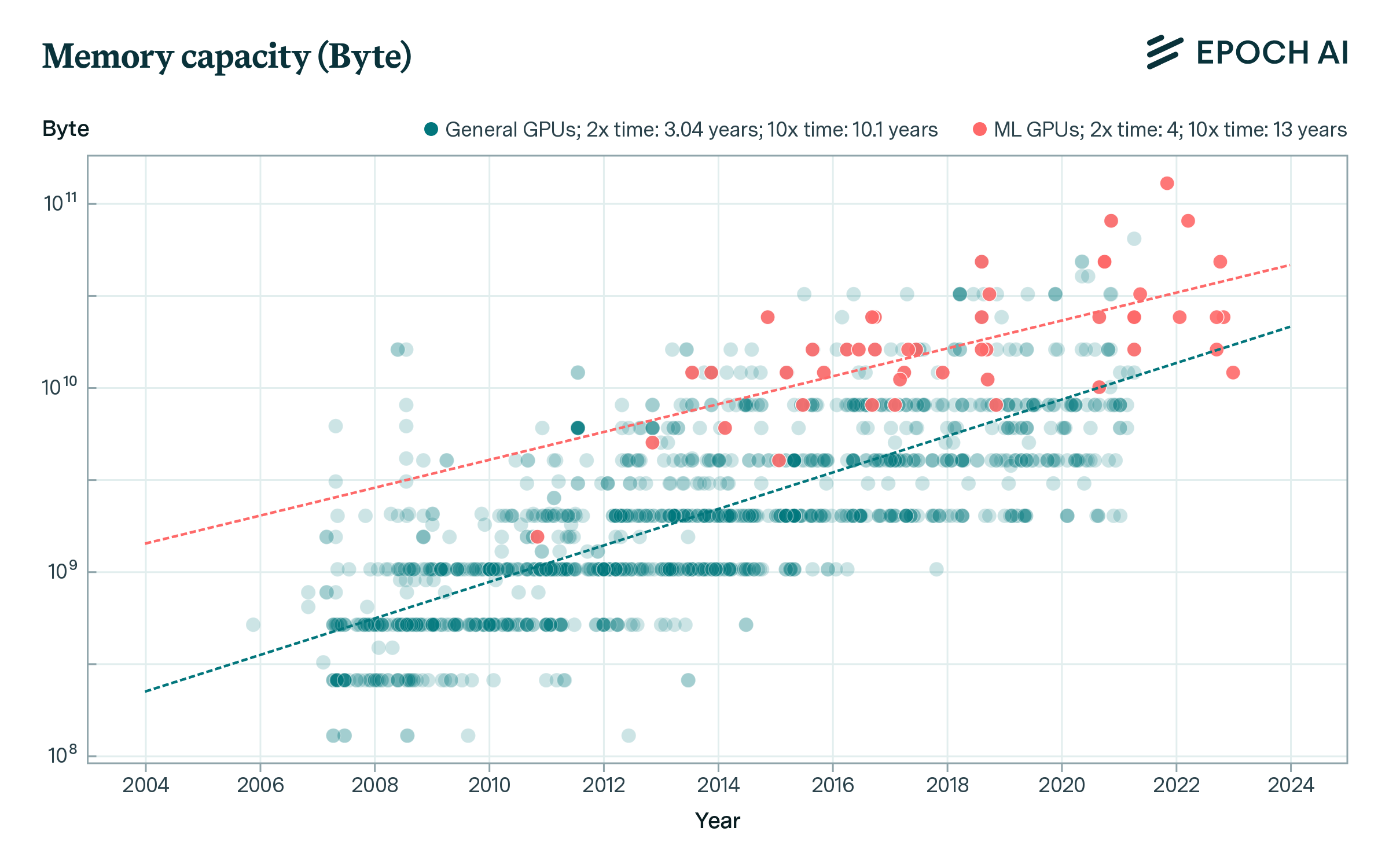
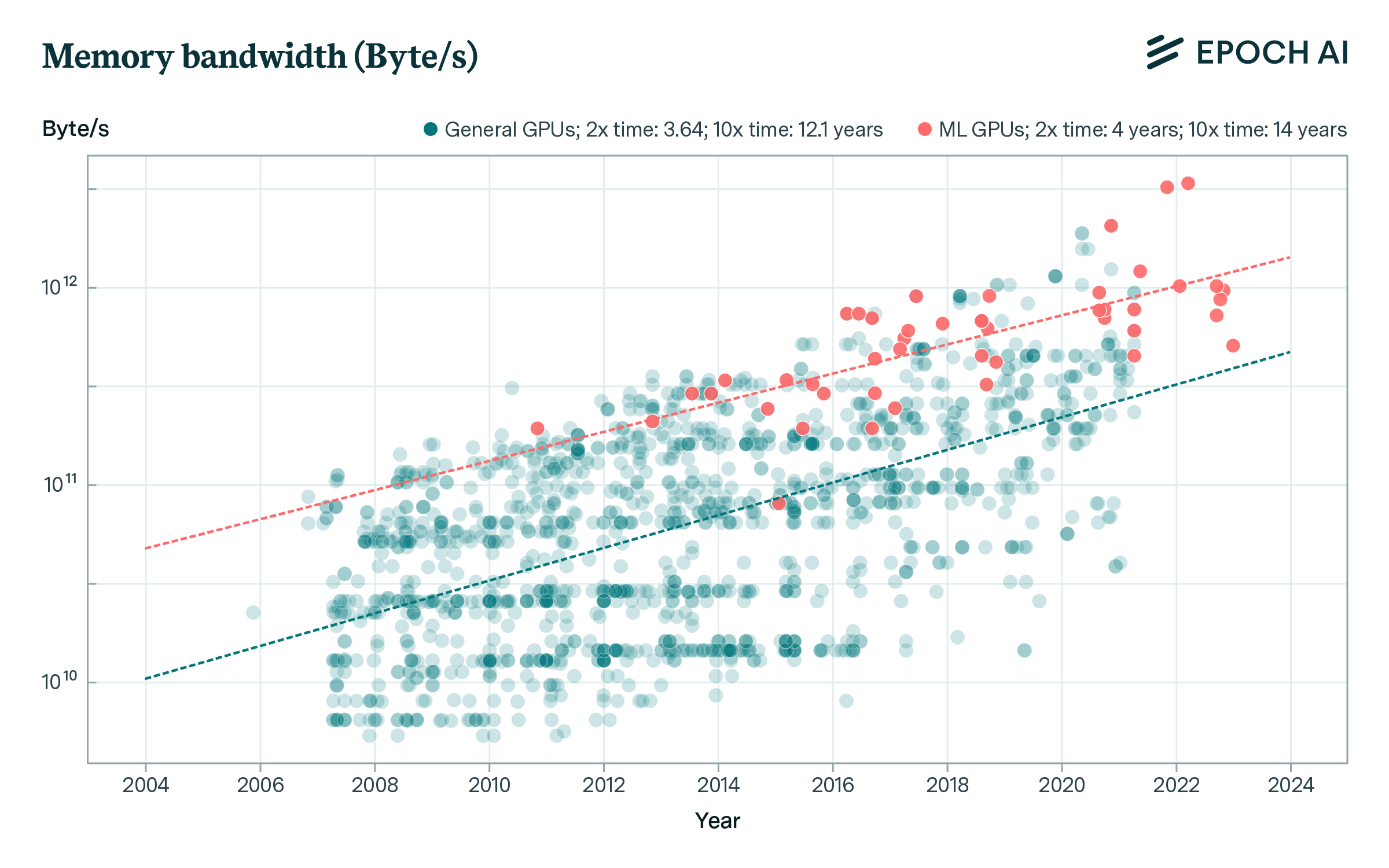
Figure 4: Trajectory of memory capacity and bandwidth for general and ML hardware. We find that all trends are slower than the trend for computational performance (doubling every 2.34 years) which is consistent with the trend often referred to as the memory wall.
As one might expect, ML hardware surpasses the median GPU in terms of both memory capacity and bandwidth. Nevertheless, here too, the growth rate for these metrics consistently trails that of the computational performance (doubling every 2.3 years). This trend suggests that memory is an increasingly critical bottleneck for large-scale ML applications. Current architectural enhancements like the introduction of number representations with fewer bits may lessen this memory constraint. However, without accelerated progress, this memory bottleneck will continue to impact overall performance in the coming years.15
A single accelerator may provide sufficient computational performance for some ML workloads. However, memory constraints frequently necessitate distributing the workload across multiple accelerators. Using multiple accelerators increases total memory capacity, allowing large models and datasets to fit in memory. This strategy ensures larger memory capacity to accommodate the entirety of a model’s weights on multiple hardware accelerators, thereby mitigating the latency incurred during data transfer from the host system’s memory. For some workloads increasing the memory bandwidth could be crucial to meet the latency and throughput requirements. Notably, techniques aimed at reducing the memory footprint, such as recomputing activations, leverage computational resources to offer a partial counterbalance to these constraints (Rajbhandari et al., 2021). Nevertheless, parallelizing the model training over multiple chips requires efficient communication between them via interconnects.
Interconnect bandwidth
In addition to the immense computational power requirements, the scaling memory needs in ML training and deployment often necessitate the use of multiple chips to satisfy these demands (for example, 6144 chips were used for the training of PaLM (Chowdhery et al, 2022) and likely significantly more for GPT4). This requirement emphasizes the need to interconnect these chips effectively – allowing them to exchange activations and gradients efficiently without offloading to CPU memory or disk.
Interconnect bandwidth refers to the peak bit rate that a communication channel can transport, measured in bytes per second. This measure becomes a limiting factor when there is frequent data exchange across ML hardware, and the interconnect bandwidth cannot keep up with the processing rate.
The maximum interconnect bandwidth is defined by the interconnect protocol. For the ML hardware in our dataset, we find three common protocols: a) PCI Express (PCIe), b) Nvidia NVLink, and c) Google Inter-Core Interconnect (ICI).16 PCIe, a ubiquitous protocol, facilitates the local interconnect between CPU and ML hardware. Nvidia’s proprietary NVLink overcomes PCIe’s bandwidth limitations by implementing direct point-to-point links between devices compared to PCIe’s hub-based network architecture. Where a point-to-point connection to a device is not available, PCIe is used as a fallback. Google’s ICI is used to interconnect their TPUs.17
Previously mentioned interconnect protocols are mainly designed for near-range communication.18 For longer distances traditional computer networking protocols, such as Ethernet or InfiniBand, are used. For all of these traditional networking protocols, the data is routed via PCIe to the networking hardware.19 PCIe serves as the standard interconnect protocol between the host CPU and ML hardware, even if NVLink and ICI are present. In the following, we always indicate the interconnect speed that corresponds to the fastest protocol available.
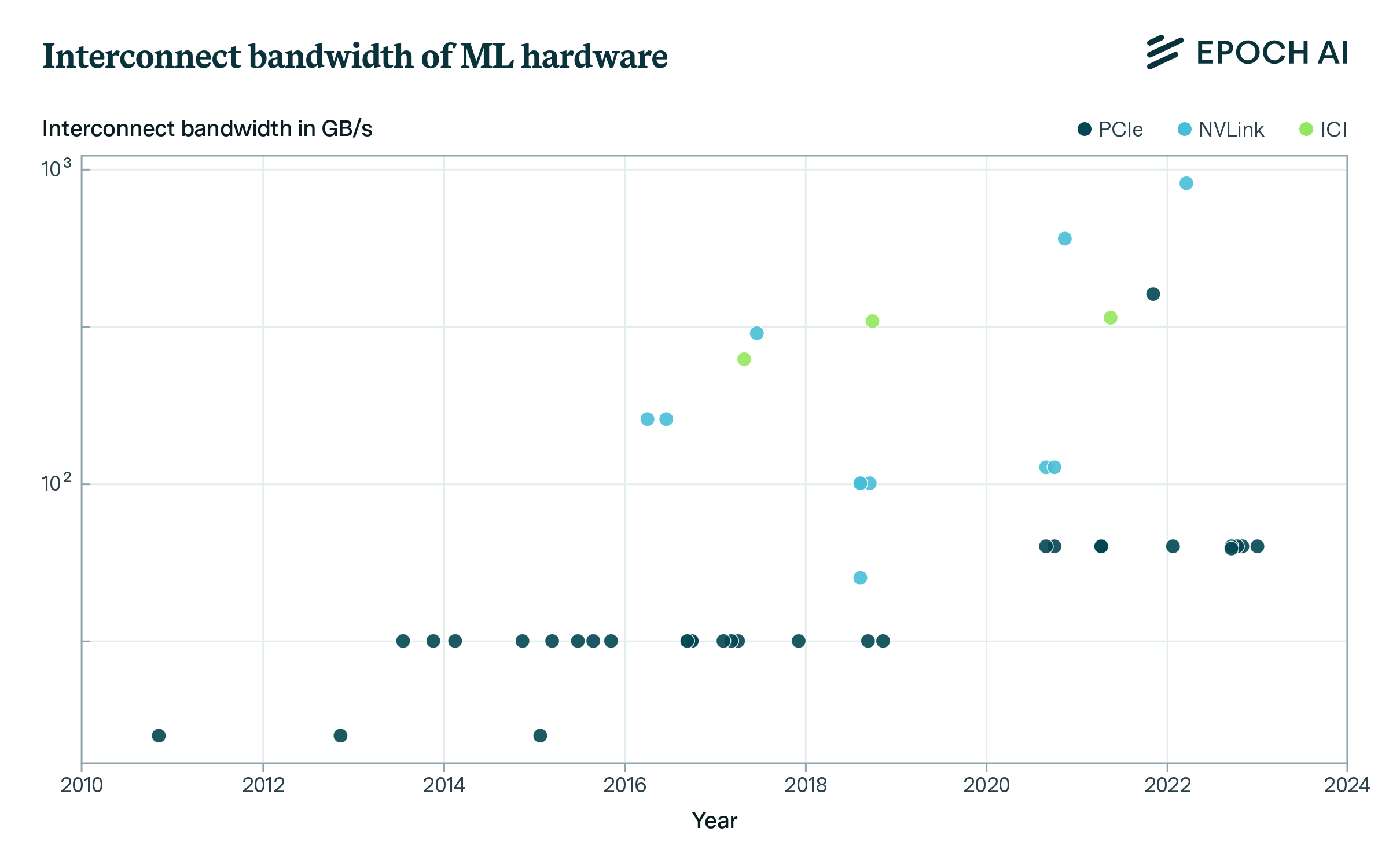
Figure 5: Aggregate interconnect bandwidth per chip for different hardware accelerators. Proprietary protocols such as NVLink and ICI have higher interconnect bandwidth than PCIe.
We find that the PCIe bandwidth of ML hardware has only increased from 32 GB/s in 2011 to 128GB/s in 2023 (Figure 5).20 However, dedicated accelerator interconnect protocols of Nvidia (NVLink) and Google (ICI) allow for higher interconnect bandwidth. Furthermore, high-end ML accelerators that are commonly used in large compute clusters (e.g., TPUs and V/A/H100) have by far the highest interconnect speed. For example, Nvidia H100 featuring 18 NVLink 4.0 links achieves 900 GB/s, which is 7x the bandwidth of a single PCIe 5.0 16-lane link.21
A compute cluster may feature thousands of hardware accelerators with different degrees of coupling. For example, the Nvidia DGX H100 server interconnects each of the eight H100s using NVSwitch, which enables a tightly coupled accelerator network at the maximum interconnect bandwidth of 900 GB/s (Choquette, 2023, section Scaling Up and Out). Many DGX H100 servers can be in turn organized in a so-called SuperPOD where the accelerators in separate servers can still transfer data using NVLink but are less tightly coupled. Each SuperPOD connects to another SuperPOD using Ethernet and Infiniband. The network topology between servers also affects the overall performance of a cluster.
Specialized cluster ML hardware has much higher interconnect bandwidth than consumer hardware. This shows its importance for large-scale ML experiments since these require high bandwidth data communication between ML hardware nodes. Therefore, similar to memory capacity and bandwidth, we suggest interconnect bandwidth should be monitored as a relevant additional metric to understand ML hardware trends.
Computational price-performance
Price-performance ratio is often a more useful metric than peak computational performance alone, as it encapsulates the overall technological improvements in GPUs—specifically, how much more performance can be attained per dollar spent. We use two approaches to estimate the price-performance of ML hardware:
- Whenever available, we use the release price of the hardware, adjust it for inflation and assume a two-year amortization time as detailed in Cotra (2020).
- In cases where a release price is unavailable or ambiguous, e.g., for TPUs or other hardware that are only available for rent, we use the cloud computing price from Google Cloud (snapshot on July 3, 2023). We adjust for inflation such that prices are comparable to the amortized prices and we assume a 40% profit margin22 for the cloud provider. When we compute the price-performance for FP32 precision as shown in Figure 6. There are several important caveats to consider when estimating FP32 price-performance. First, pricing for cluster hardware is often negotiated privately rather than publicly listed, making accurate pricing difficult to determine. Second, some chips may have insufficient interconnect bandwidth or reliability to be used in industrial cluster deployments, despite having strong individual price-performance. Third, the FP32 calculation introduces bias against specialized ML chips which utilize lower precision number formats and tensor cores not reflected in FP32 metrics. Finally, estimating real-world maintenance costs is challenging given the lack of published data on quantities like power, cooling, and replacement rates (see Cottier, 2023). While useful as a baseline, FP32 price-performance trends must be considered in the context of these limitations stemming from ML-specific architectural factors and data constraints.
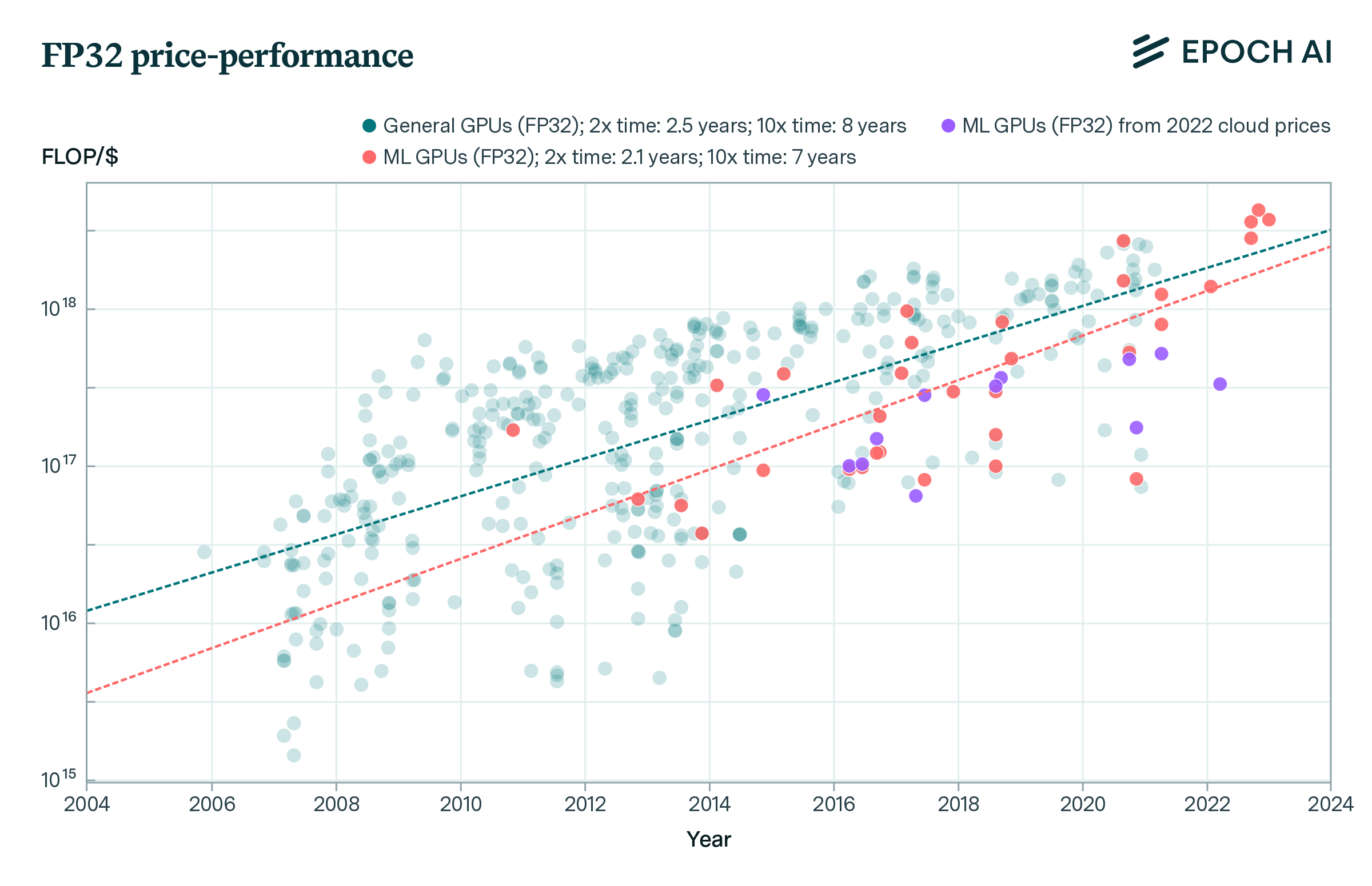
Figure 6: Trajectories of FP32 price-performance for general and ML hardware. We find that the trajectories roughly follow the same growth trajectory as peak computational performance (2.3 years doubling time). Furthermore, we find that ML GPUs have lower absolute price-performance than other hardware. FP32 price-performance may be biased against ML hardware (see text).
We see that the growth trajectory of FP32 price-performance (2.5/2.1 years doubling time) approximately follows that of general computational performance (2.3 years doubling time).
Furthermore, we find that price-performance is historically lower for ML GPUs compared to the other GPUs. We speculate that there are at least two reasons for this. First, the caveats presented above systematically bias FP32 price-performance against ML hardware since they ignore other number representations like FP16 that are common in ML training. Second, as described in the previous sections, large scale ML training relies not on a single performance metric but many, such as interconnect bandwidth, memory capacity, and bandwidth. However, these metrics are not reflected in the FP32 price-performance. For example, a typical consumer GPU might have better price-performance individually but is much less appropriate for ML training.
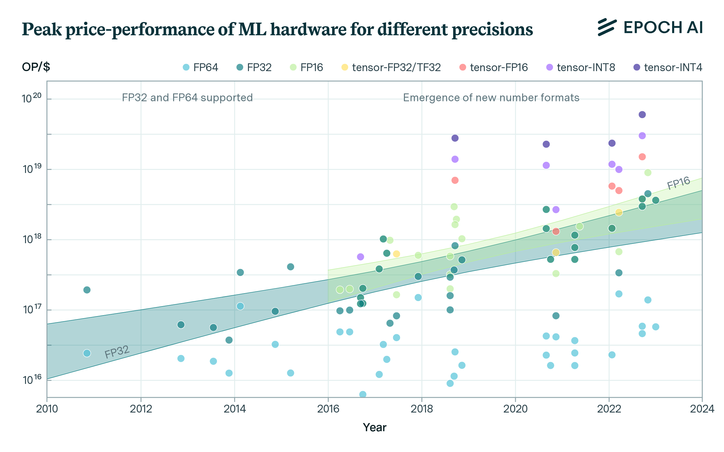
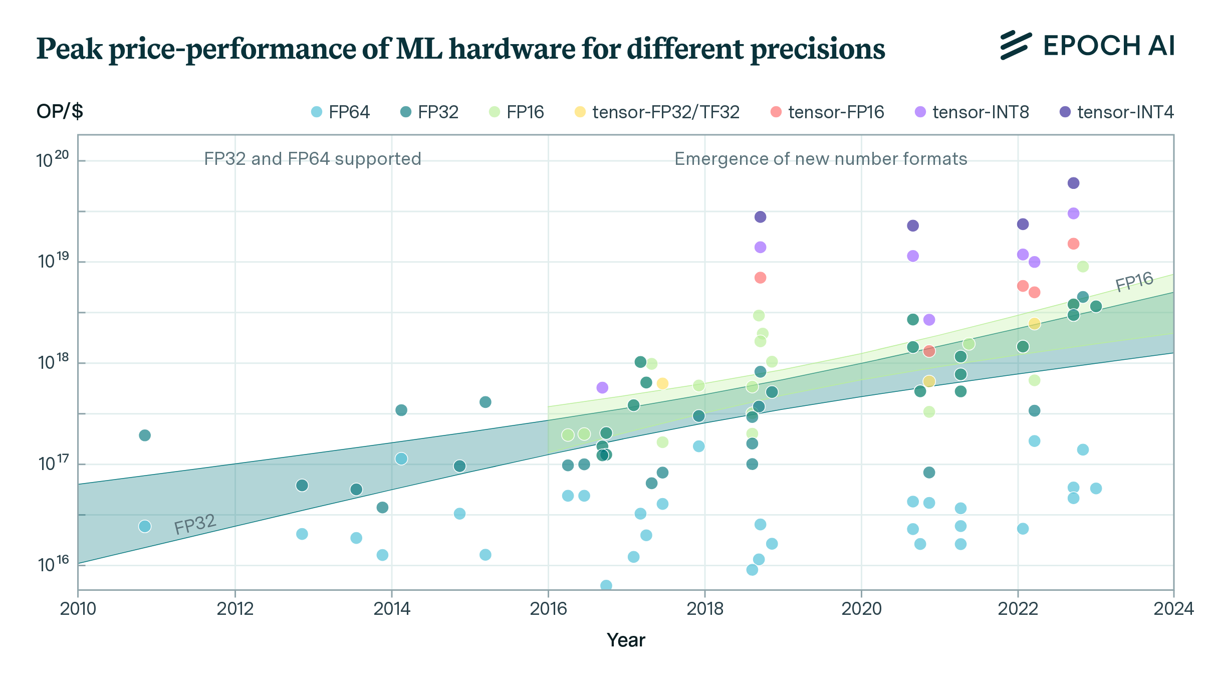
Figure 7: Computational price-performance of ML hardware for different number representations. Points illustrate the release date and performance of ML hardware, colored by number format. Dashed lines indicate the trends in performance improvements for number formats with ten or more accelerators: INT8, FP16, and FP32.
FP32 price-performance can misrepresent cost-effectiveness for ML hardware. For example, the AMD Radeon RX 7900 XTX consumer GPU has the best FP32 price-performance. However, the NVIDIA RTX 4090 delivers approximately 10 times higher price-performance when using low-precision INT4 formats common in ML training. This is enabled by the RTX 4090’s tensor cores specialized for low precision calculations, which FP32 metrics overlook. Consequently, FP32 price-performance alone would incorrectly identify the Radeon as superior, when the RTX 4090 is actually far more cost-effective for real-world ML workloads. This demonstrates the risks of relying solely on FP32 price-performance analysis, rather than a holistic evaluation accounting for ML-specific architectures and number representations.
The GPU with the best price-performance depends heavily on the number representation used. For FP32 calculations, the AMD Radeon RX 7900 XTX consumer GPU has the highest price-performance. However, for lower precision number formats like INT4, the NVIDIA RTX 4090 is approximately 10x better in terms of operations per dollar. This illustrates how ranking GPUs by price-performance is highly sensitive to precision, and FP32 alone does not capture cost-effectiveness for real-world ML workloads.
Energy efficiency
Running hardware consumes energy, and most organizations aim to utilize their hardware as much as possible. Thus, deploying energy-efficient hardware is a possible way to reduce cost over the lifetime of a hardware accelerator. Furthermore, more energy-efficient hardware typically dissipates less heat which allows for better scalability.
To approximate the energy efficiency of ML hardware, we use FLOP/s per Watt, where the energy component is computed from thermal design power (TDP). TDP is not equivalent to average energy consumption and it should not be used for exact comparison. However, in the context of ML training and cloud computing, we think it is a reasonably good approximation since the hardware is operating non-stop (see TDP section in the appendix).
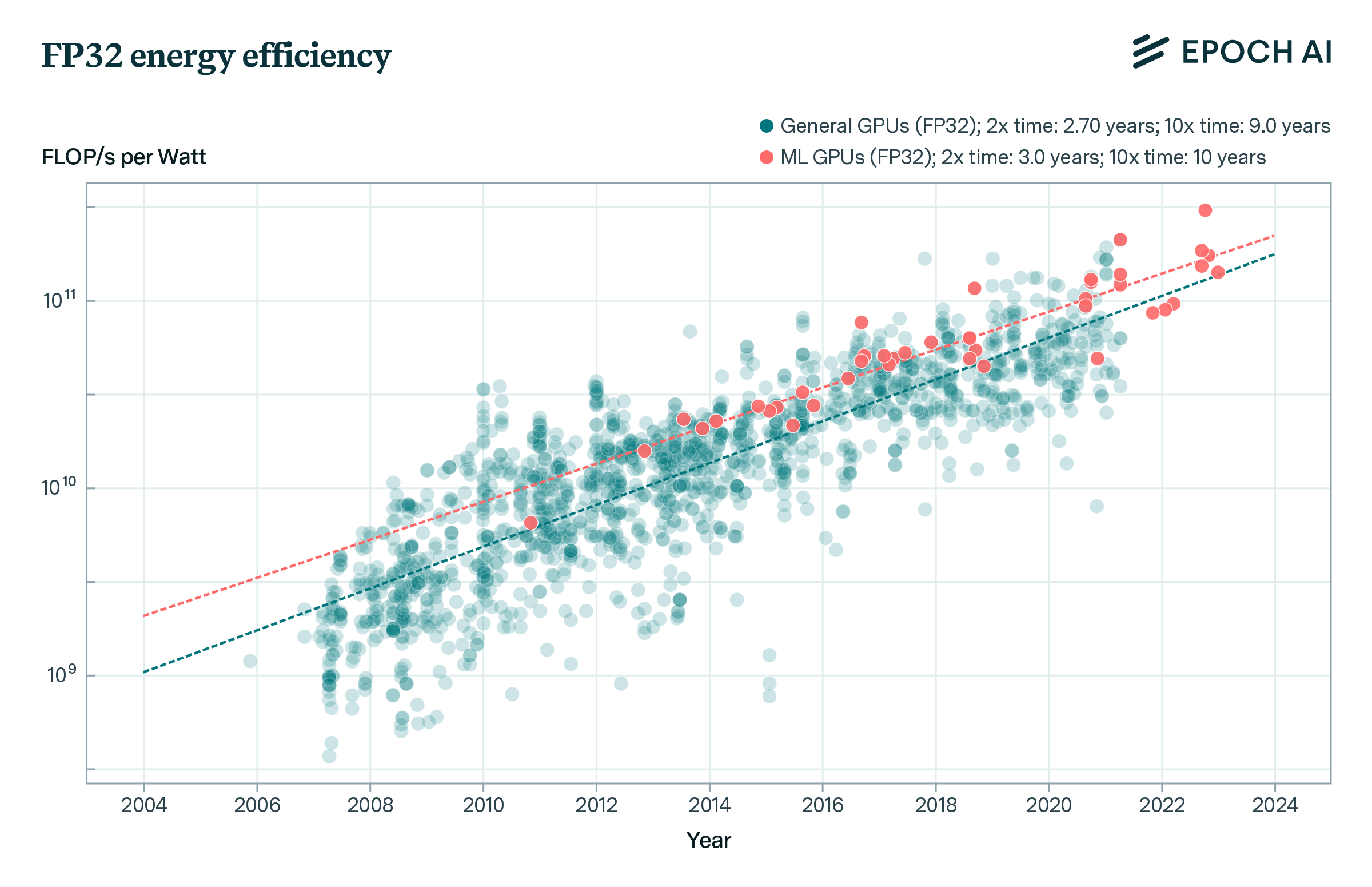
Figure 8: Trajectory of energy efficiency for FP32 precision computed from TDP values. We find that ML GPUs are, on average, more energy efficient than general GPUs and that energy efficiency grows slightly slower than peak computational performance (2.3 years doubling time).
We see that ML GPUs are on average more energy efficient than historical GPUs. This is plausible since ML GPUs are usually running in data centers, where energy consumption and carbon footprint are important metrics (see e.g., Jouppi et al., 2023, section 7.6). Furthermore, we find that the growth rate of energy efficiency (2.70/3.0 years doubling time for historical and ML GPUs, respectively) is only slightly slower than that of peak computational performance (2.3 years doubling time). This trend suggests that energy consumption is not (yet) a realistic bottleneck to scaling, but there are reasons to assume it could be in the future (Hobbhahn & Besiroglu, 2022b).
Conclusions
Recently it has been shown that low precision is sufficient for both developing and deploying ML models (Dettmers et al., 2022; Suyog Gupta et al., 2015; Courbariaux et al., 2014). We find that ML hardware follows these findings and continuously integrates hardware units for lower precision number formats like FP16, TF32, BF16, INT8, and INT4 to increase the total number of operations per second. Furthermore, specialized computation units such as tensor cores become increasingly common and further increase computational performance. Combining both trends, in our very speculative estimates, the jump from FP32 to tensor-FP16 provides an ~8x increase in peak performance on average. However, flagship ML hardware accelerators can have even larger ratios, e.g., the NVIDIA H100 SXM has a TF32-to-FP32 ratio of ~7x, a tensor-FP16-to-FP32 ratio of ~15x, and a tensor-INT8-to-FP32 ratio of ~30x.
This trend suggests a type of “hardware-software co-design,” where ML practitioners tinker with different number representations and already get a small but meaningful benefit from increased performance and decreased memory usage. Then, the hardware is adapted to these new number representations to reap further benefits. Multiple iterations of this cycle can lead to substantial improvements in performance. Additionally, hardware producers are actively looking for new innovations themselves which then lead their way into the ML labs.
Furthermore, we emphasize the importance of factors like memory capacity, memory bandwidth, and interconnect bandwidth for large-scale ML training runs. Given that modern ML training runs require the efficient interaction of often thousands of chips, factors beyond peak per-chip performance become crucial. We observe that these metrics grow at a slower pace than compute-related metrics (e.g., peak computational performance, price-performance, and energy efficiency). Memory and interconnect bandwidth are a bottleneck for the utilization of peak computational performance in large distributed ML training scenarios.
Specialized machine learning hardware and alternate number representations are relatively new trends, making precise predictions difficult. As we have made clear, closely tracking developments in number formats, memory capacity, memory bandwidth, and interconnect bandwidth is crucial for yielding more accurate assessments of future machine learning capabilities. Rather than relying on static assumptions, constantly reevaluating performance potential based on hardware and software innovations is key.
We would like to thank Dan Zhang, Gabriel Kulp, Yafah Edelman, Ben Cottier, Tamay Besiroglu, Jaime Sevilla, and Christopher Phenicie for their extensive feedback on this work. We’d like to thank Eduardo Roldán for porting the piece to the website.
Appendix: Trends of secondary performance metrics
We supplement our work with trends of secondary metrics like number of transistors, TDP, clock speed, die size and number of tensors cores. Even though these metrics might be relevant to understand some trends in ML hardware, we think they are less important or less influential23 than the metrics we analyzed in the body of our article.
Note that many of these trends have a lot of missing data and might thus be biased. For example, most of the following data do not include TPUs.
| Unit | Number of datapoints | Trend | Increase | Datapoint of highest performance |
| Number of transistors | 42 | exponential | 2x every 2.89 [2.49; 3.33] years 10x every 9.58 [8.26; 11.07] years 0.104 [0.121; 0.090] OOMs per year | ~8e4 (NVIDIA H100 SXM) |
| Die Size in mm² | 42 | linear | slightly increasing | 1122 (NVIDIA Tesla K80) |
| TDP in Watt | 43 | linear | unclear | ~7e2 (NVIDIA H100 SXM) |
| Clock speed in MHz | 42 | linear | no significant change | ~2.2e3 (NVIDIA GeForce RTX 4070) |
| Number of shading units / cores | 42 | exponential | 2x every 3.41 years 10x every 11.33 years 0.088 OOMs per year | ~1.81e4 (NVIDIA L40) |
| Number of tensor cores | 23 | not applicable | no trend visible | ~6.4e2 (NVIDIA Titan V) |
Number of transistors
Figure 9: Development of the number of transistors. We find that the growth rates are slightly slower than peak computational performance (doubling every 2.3 years).
The number of transistors follows a very similar pattern as the peak performance, i.e., ML hardware and general hardware have a very similar growth rate but different absolute values. The growth rate of the number of transistors is slower than peak computational performance (2.3 years doubling time) which indicates that computational performance cannot be fully reduced to the number of transistors.
Die size
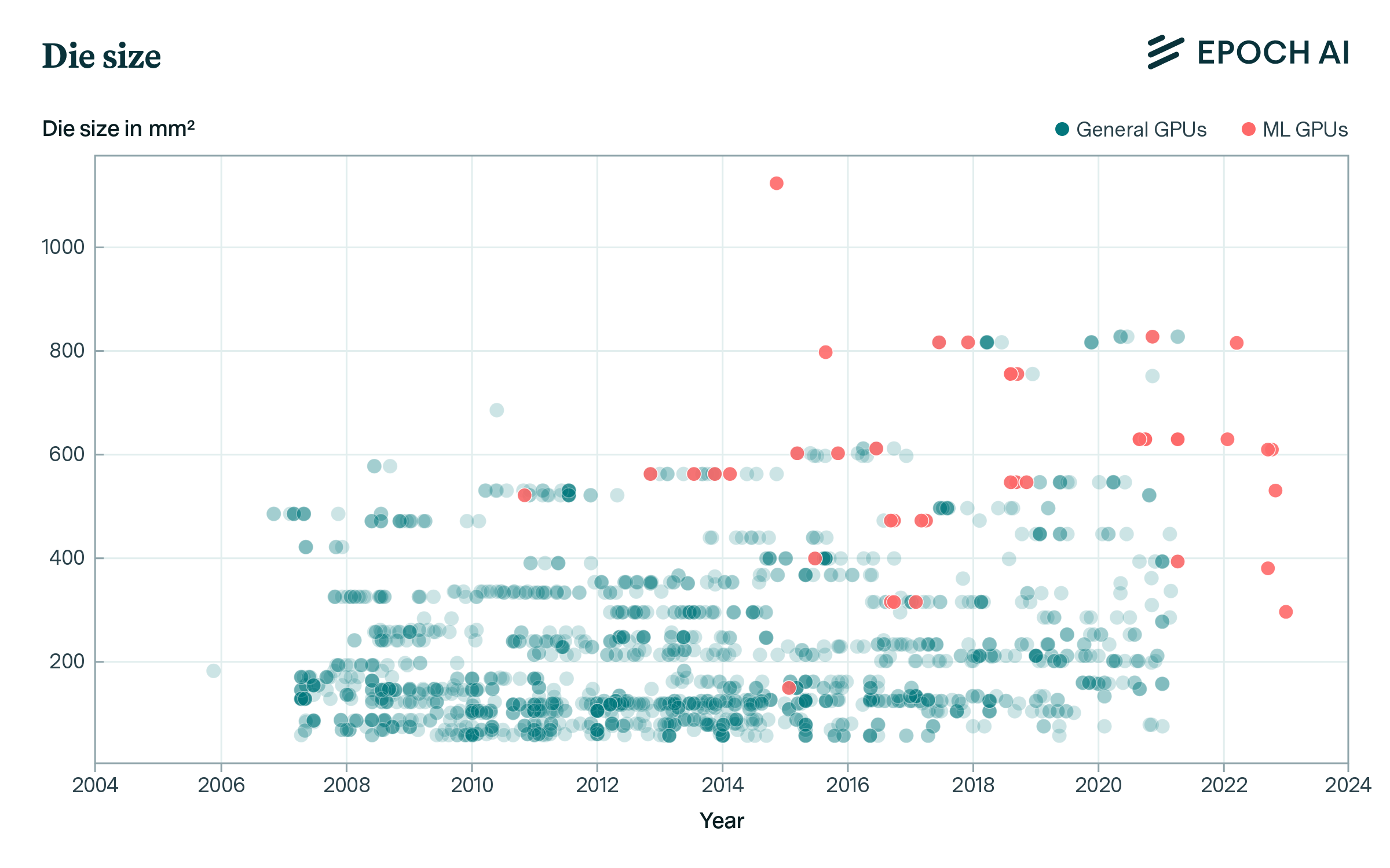
Figure 10: The largest dies are limited at 858 mm² by the EUV reticle limit. On average, ML hardware dies are among the larger ones and there might be a slight increase in overall size.
A processor package integrates typically a single or many interconnected dies.24 A larger die can integrate more logic and thus enables more compute resources that can be interconnected with a high bandwidth on a single chip, however, enlarging the die size typically decreases the ratio of functional chips during manufacturing. The die size has only slightly increased over the last 15 years until it reached the EUV reticle limit of 858 mm²., indicating that a) the industry could not find new solutions to increase the die size, or b) increasing the die size is not the only way to increase performance. Nonetheless, ML hardware tends to be among the biggest hardware accelerators, likely to maximize computational performance per chip. Vice versa, semiconductor manufacturers tend to use flagship chip designs to improve their processes, including die size.
Thermal design power (TDP)
All energy consumed by a chip must be dissipated as heat, which in turn must be carried away by a cooling system to avoid overheating. TDP is the thermal power that a cooling system should be able to carry away and is a requirement provided by the chip designer. The peak power is often higher than the TDP but the average power consumption will be lower.25 TDP may be defined for a single chip or a computer expansion card comprising many chips and additional circuitry. Moreover, TDP is based on safety margins, which may differ among chip designer companies. In the context of ML hardware, this can be seen as an approximation of the energy consumption, assuming most ML hardware runs at maximum capacity.26 As TDP calculation may differ among chips from different chip designers, this metric should not be used for exact comparison.
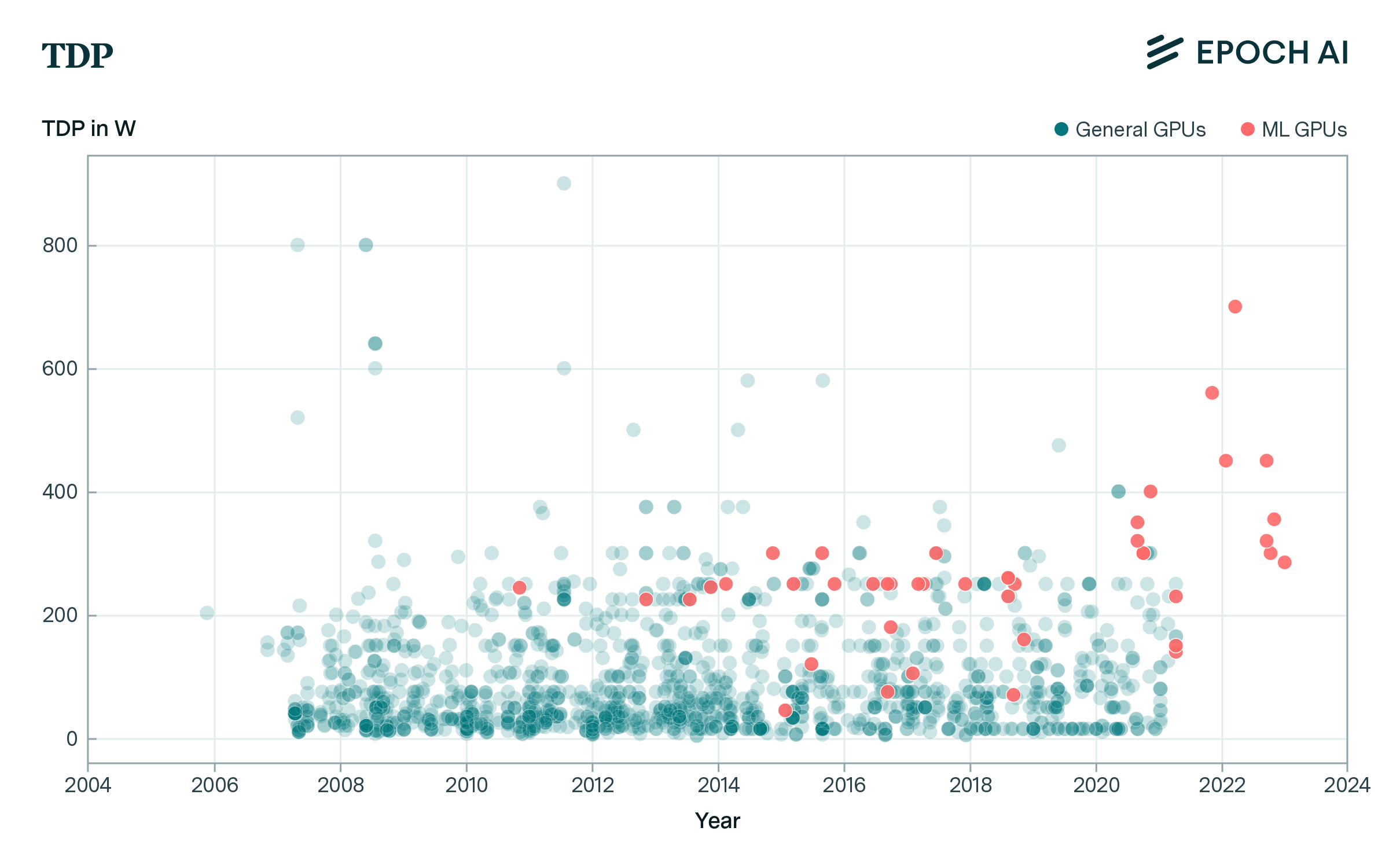
Figure 11: We find that there is no clear trend in TDP over the last two decades. Potentially, there is an increase in TDP for the latest ML GPUs.
TDP has not changed substantially over the last 15 years. The latest ML hardware models seem to have a higher TDP than previous models, but we should be very careful not to overinterpret a few datapoints due to the non-standardized definition of TDP. In general, we are unsure about whether there is a meaningful trend with TDP or not.
Clock speed
New semiconductor manufacturing processes typically allow more logic components per die area and shorter distances between the logic components. This enables higher clock speeds, which in turn leads to more power consumption and heat that has to be transferred away from the chip. The factors limit the maximum frequency on a single chip.
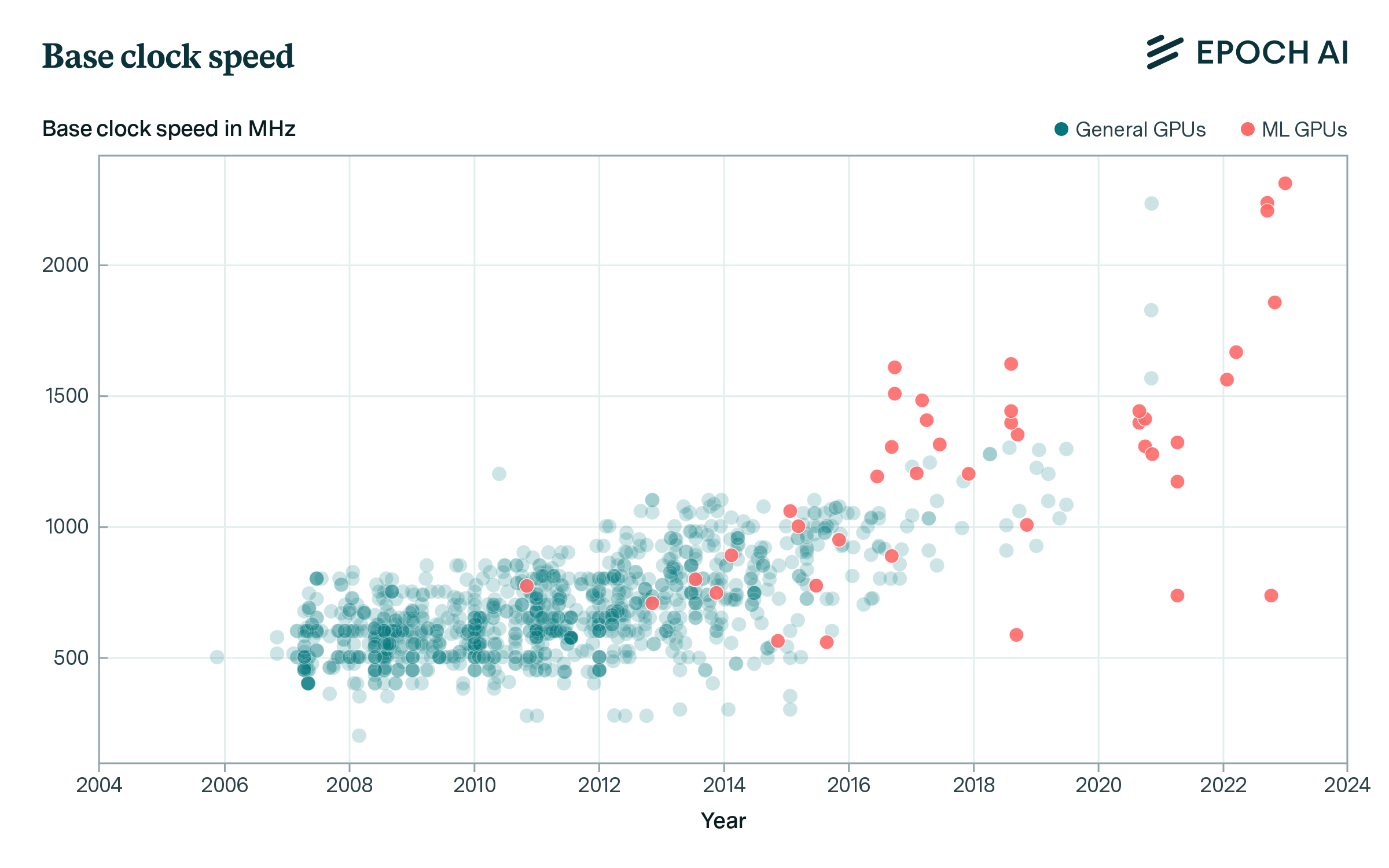
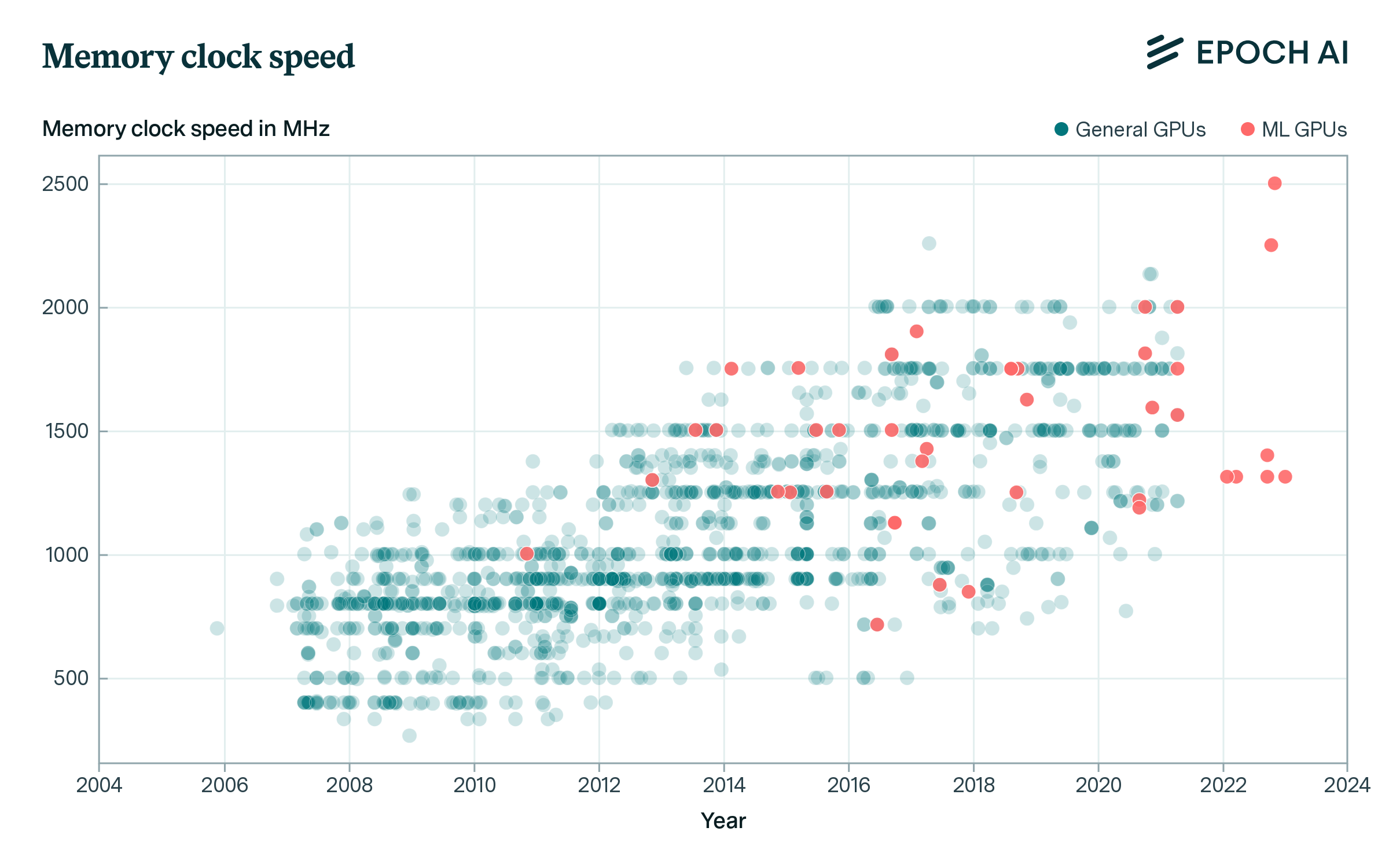
Figure 12: We find a very slow but steady increase in GPU base and memory clock speeds over the last two decades. However, the overall improvement of ~4x over more than 15 years indicates that clock speed is only a minor driver of overall computational performance progress.
The overall improvement of ~4x over more than 15 years indicates that clock speed is only a minor driver of overall computational performance progress.
Number of shading units/CUDA cores
In theory, shading units and CUDA cores are two slightly different things. Shading units are used to render graphics-specific operations while CUDA cores are an NVIDIA-specific term that refers to general-purpose units. Both shading units and CUDA cores are highly parallel. In the context of ML, we can think of shading units as nearly equivalent to CUDA cores since both are used to speed up matrix multiplications.
Unfortunately, different manufacturers use different terms, and the two types of units might not be exactly equivalent. In our work we consider shading units and CUDA cores to be functionally equivalent.
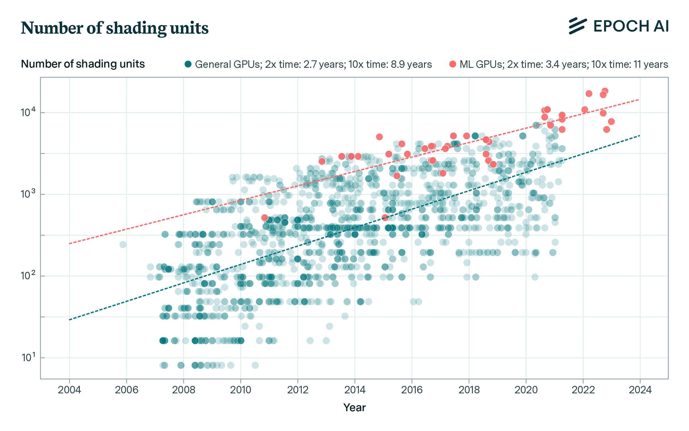
Figure 15: We can see a clear trend in the development of the number of shading units (~CUDA cores) that approximately shadows that of general computational performance (doubling time 2.34 years).
We find that the number of shading units/cores steadily increased over the last 15 years at a lower speed (doubling every 3.4 years) than peak computational performance (doubling every 2.3 years).
Number of tensor cores
Since ~2017, hardware manufacturers have experimented with tensor cores, i.e., units that are designed for matrix multiplications. Tensor cores differ from CUDA cores or shading units because tensor cores are more specialized and can perform less general-purpose computations.
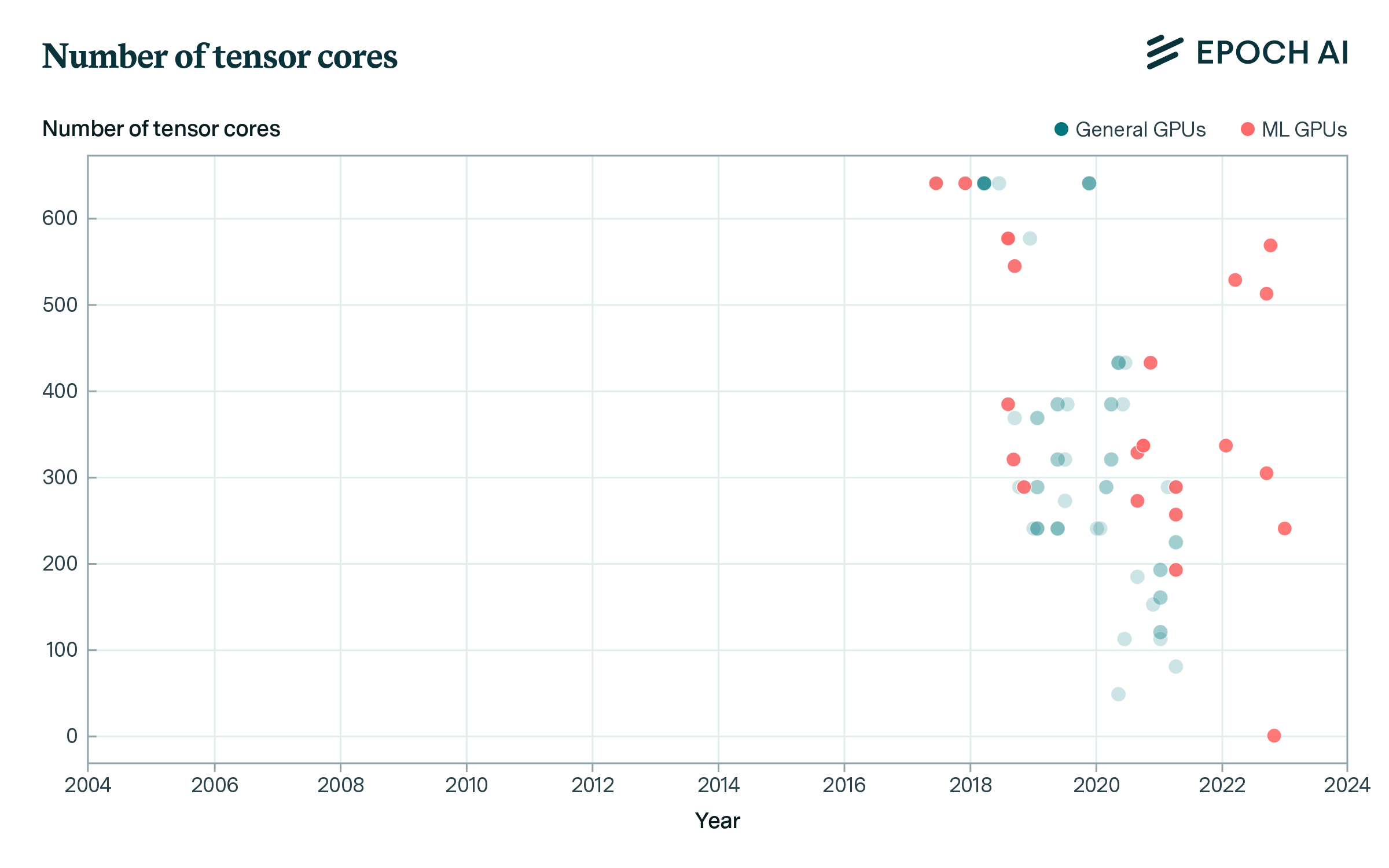
Figure 16: We cannot see a clear trend in the development of the number of tensor cores.
Since then, there has been no clear trend in the number of tensor cores. Despite this, we expect that the performance of tensor cores has increased. For example, NVIDIA H100’s tensor cores can have a speedup between 1.7 and 6.3 compared to its predecessor A100.
Therefore, we suggest that merely tracking the number of tensor cores is the wrong approach and we should rather look at the overall computational performance of all tensor cores on a chip combined and adjust for total utilization.
Notes
-
NA means not available, and is the result of a lack of sufficient data to reliably estimate the relevant growth rates. ↩
-
These numbers are often calculated based on hardware features. For example, the computational performance is often estimated as the product of a) number of processing cores, b) clock speed and c) floating-point operations per clock cycle per core. ↩
-
The same amount of bits can represent different number ranges or floating-point number precisions. Our hardware dataset does not include the computational performance for every available number format for a given bit-length. For example, our FP16 data also includes BF16 which differ in the number of allocated bits to the exponent and fraction. We do not expect much performance difference between different floating-number formats of the same bit length. The most suitable number representation (e.g., in terms of energy- or runtime-efficiency) depends on the workload. Rodriguez, 2020, Section 6.1 also includes a comprehensive list of number representations for ML applications. ↩
-
According to Table VI in Mao et al. (2021), an FP64 multiplier unit takes roughly five times the area of a FP32 multiplier. Similar relation exists between an FP32 and FP16 multiplier. ↩
-
Due to the high precision requirements of many historically important supercomputer workloads, such as computational fluid dynamics, meteorology, nuclear Monte Carlo simulations, protein folding, etc. ↩
-
Rodriguez, 2020, Section 6.1 states: The most popular and widely adopted number format is FP32 for both training and inference. The industry is moving toward FP16 and BF16 for training and inference, and for a subset of workloads, INT8 for inference. ↩
-
TF32 is not a general-purpose number format. It is only used in NVIDIA tensor cores and speeds up the processing of models using FP32 by cutting down 13 precision bits before matrix multiplication but keeping the same number range as FP32. TF32 has the same memory footprint as FP32, as TF32 uses the same registers as FP32 in tensor cores (Sun et al., 2022, Section 8). In other words, TF32 was designed as a drop-in replacement for models that use FP32 but can accept less precision during matrix multiplication. ↩
-
Not to be confused with the new instructions required for tensor-core multiplication. Choquette et al., 2021, section SM Core states: In A100, a new asynchronous combined load-global-store-shared instruction was added which transfers data directly into SMEM, bypassing the register file and increasing efficiency. ↩
-
See especially the section titled ‘SM Core’. ↩
-
For example, INT8 is currently not widely used for training current systems. INT8’s drawbacks are explained in Rodriguez, 2020, Section 6.1. ↩
-
Memory capacity documented by the ML hardware datasheet usually refers to the RAM capacity, often also referred to as video RAM (VRAM) given the historical connotation of GPUs being used for video processing. ↩
-
For example, AMD Instinct MI200 datasheet explicitly states 128 GB HBM2e. HBM refers to high-bandwidth memory which is a type of RAM. NVIDIA H100 Tensor Core GPU Datasheet states 80 GB of memory for H100 SXM and according to NVIDIA H100 Tensor Core GPU Architecture, v1.04, p36 this number corresponds to HBM3 memory capacity. ↩
-
The actual bandwidth in an application will typically be lower. One reason is the data transfer latency which depends also influences the actual bandwidth and depends on the memory technology. The distance to a separate memory chip and long paths inside a large memory additionally lead to a high number of cycles before the bits arrive at the processing unit. If the processing unit knows which data is required beforehand, then data transfer at the peak bandwidth is possible. If not, random accesses to the memory are required. Typically the more random the accesses, the less the actual bandwidth. We don’t cover latency metrics in our dataset. ↩
-
Graphics processing and ML training tend to have this bottleneck, so modern ML hardware tries to optimize high memory bandwidth by using two technologies: (a) GDDR memory or (b) high-bandwidth memory (HBM). GDDR memory is featured on the same board as the processing chip, whereas HBM is implemented in the same package as the processing chip, allowing for lower latency and higher bandwidth (for example, cutting-edge ML accelerators used in data centers, such as the NVIDIA A100 and H100 feature HBM; whereas their gaming GPUs do not feature HBM to save costs). Stacking many DRAMs together and interconnecting many semiconductor dies in a single chip package requires expensive tools compared to connecting a processing chip with a DRAM on a printed circuit board, so HBM is commonly featured in the most expensive and performant ML hardware accelerators, such as those used in data centers for large-scale ML training and deployment. ↩
-
See Megatron-LM: Training Multi-Billion Parameter Language Models Using Model Parallelism, How to Train Really Large Models on Many GPUs? or Techniques for training large neural networks ↩
-
Details in section 2 of Jouppi et al., TPU v4: An Optically Reconfigurable Supercomputer for Machine Learning with Hardware Support for Embeddings, 2023 ↩
-
More info on ICI see Jouppi et al., 2023, Section 2. Notably TPUv4 uses optical switches to cater for the long interconnect links. ↩
-
For example, PCIe 4.0 supports up to 30 cm. According to Jouppi et al., 2023, Section 7.2, Google ICI is to interconnect 1024 TPUv3s, however maximum length is not provided. ↩
-
InfiniBand and Ethernet support a lower network bandwidth than PCIe, so they define the peak bandwidth. ↩
-
As standardized by the PCI-SIG consortium; with an expected increase to 256 GB/s by 2025. Note that the pace at which this bandwidth changes is defined by the consortium, and the consortium may be slow at adopting the immediate needs of the market. ↩
-
According to NVIDIA H100 Tensor Core GPU Architecture, v1.04, p47 states: Operating at 900 GB/sec total bandwidth for multi-GPU IO and shared memory accesses, the new NVLink provides 7x the bandwidth of PCIe Gen 5. … H100 includes 18 fourth-generation NVLink links to provide 900 GB/sec total bandwidth… ↩
-
Google Cloud offers a one-year committed use discount of 37%. Thus, we estimate that 40% is a reasonable lower bound for the profit that Google makes from normal cloud computing. More considerations on prices from cloud computing can be found here. ↩
-
The judgment of relevance is a mix of the author’s intuitions and the reasoning provided in our previous post on GPU performance predictions. ↩
-
Chiplets are an example of multiple dies in one integrated circuit/package. ↩
-
From Hennessy et al., Computer Architecture, 2017, p.24: TDP is neither peak power, which is often 1.5 times higher, nor is it the actual average power that will be consumed during a given computation, which is likely to be lower still. ↩
-
Evidence to support this comes from the Gigabyte glossary: In a stable, enterprise-grade server room or data center, the TDP roughly equates to the computing equipment’s power consumption, since the servers are usually operating at or close to maximum capacity. ↩
About the authors


Related posts